Layout Pcb Power Montarbo
• high power electronics design a plus. You can also check out the design techniques for emi reduction in smps circuits.
Pcb Layout Mixer Audio Pcb Circuits

As consumer devices continue to shrink in size become more and more portable, components inside are getting smaller but providing better performance, power, and current considerations and related thermal design become increasingly important for pcb designers and board layout engineers.

Layout pcb power montarbo. Pcb layout tips for power integrity. • experience with low noise, low emi design. Pcb power market was founded in 1996 as csil, with a vision to provide pcb services of global scale and quality, to the needs of innovators across the electronics industry.
The rjp05 is 2.4 ghz to 2.5 ghz; Start with the main components of the supply first,. 50w, ocl main amplifier —lf351, 2n3055, mj2955.
2n3055 amplifier circuit with pcb. High efficiency power stage for wlan power amplifier. By overseeing the complete process, it allows us to manage our customers' projects from the design.
Five steps to a good pcb layout of a boost converter 5. Switching power supplies the importance of a good printed circuit board (pcb) layout in switching power supplies cannot be overstated. The organizational fuel of excellence driven action has empowered our year on year growth, on the back of diligent, transparent and honest work of a phenomenal team.
For pcb system design, strong layout tools augment power plane designs. Pcb layout basics for engineers. The pcb connects electronic parts of the product to form a system.
• experience as pcb librarian. The amplifier is designed using 0.18um sige bicmos process for 802.11 b/g wlan systems. In most instances an electronics hardware design engineer will design the circuit, and then a pcb layout specialist.
The copper area to the left of the device is the power input. Venture amplifier pcb layout team has the industry leading design engineers and 10 years'amplifier pcb layout experiences. The layout is also critical for trace spacing in order meet the shock and fire safety standards.
Is a printed circuit board solution provider located in anaheim, california. Printed circuit board, pcb design, is one of the most important design elements within the design of an electronics product. From material development and production, circuit fabrication to final component assembly , venture amplifier pcb layout team has full experience in processing a wide variety of printed circuit board materials.
In this guide, we've compiled some of the essential pcb layout guidelines that apply to most modern circuit boards. The subject of pcb layout has been The single point should be closed to the pgnd pin.
This device has long pads for power, ground, and the three outputs. 50w ocl mosfet amps —using k1058 + j162. Developing the schematic and debugging the breadboard is a good start, but the final, critical challenge is to layout the pcb.
This large copper area is connected to the two power pads of the device directly. In this final section on pcb layout, we're going to look at reduced schematics from the. When it comes to actually laying out the power supply, here are a few important categories to focus on:
35w to 75w stereo amps —tda2050**new**. To keep your power routing as short as possible, keep the component placement as tight as you can. Figure 15 shows a pcb layout for an mp6540 power stage ic.
Note that the package is only 5mmx5mm. Whether you are moving at a high speed or you're designing a high speed printed circuit board, good design practices help ensure your design will work as intended and can be manufactured at volume. Imagine you are watching a movie with your family.
( 2) tambah ke wishlist. Your reliable high power pcb design partner. Sound power is very realistic with these circuits.
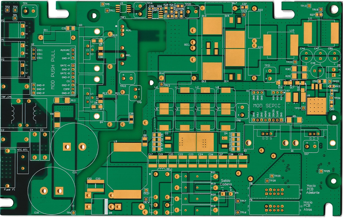
Fortunately, understanding the phenomenon behind the A power converter layout on a printed circuit board. High power pcb design (1kw, input.
Pcb super power itali 2500w montarbo fiber. Experience with rf and analog design. The layout of the pcb is critical for radiated emissions, and susceptibility to external stray fields that can cause functional failures.
Established in 2000, pwb america, inc. Pcb design basics schematic capture & drawing pcb layout / routing pcb design guidelines pcb signal integrity. Montarbo made in italy, professional sound systems, montarbo as pioneer in professional audio field, produces active and passive loudspeakers,cabinet,power.
55w rms otl integrated amps build easily. • simulation tools such as spice a plus. The geda02 is 20 ghz to 40 ghz low power.

Evatronix PCB layout design

Pin on Electronic circuit projects
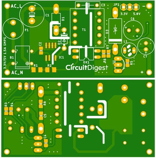
Design your own Compact 5V/3.3V SMPS Circuit for Embedded
How to do a PCB layout review Fully Charged Archives

PCB Layout SOCL BOOM TEF Driver Power Amplifire BLOGKAMARKU
Custom PCB Design Gallery for double & multilayer boards
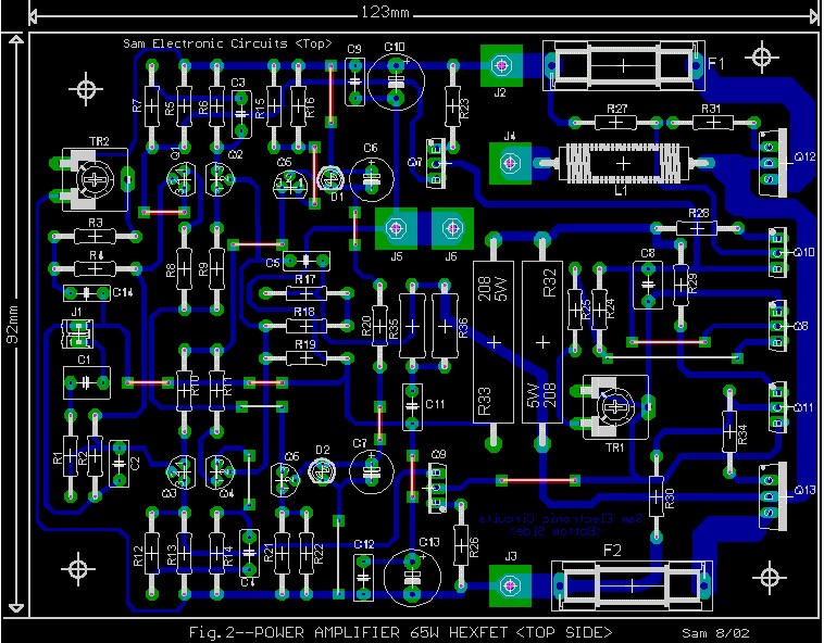
65W Power Amplifier PCB layout Electronic Schematic Diagram
PCB LAYOUT POWER MEGATECH UNTUK SOUND LAPANGAN BLOGKAMARKU
THAT Power Supply

Dual Adjustable DC Power Supply

Layout PCB Driver Power TBM DUAL INPUT BLOGKAMARKU

Turnkey PCB & PCBA Manufacturing What's The Difference
Making your first Circuit Board Getting started with

PCB Layout Design Electronic Circuit Electronics

PCB Layout [DIPTRACE] YouTube

Make Sure to Consider These Factors When Creating a PCB

3kW Power Amplifier Driver Circuit PCB Layout Electronic
PCB Layout Style Mistakes That Can Ruin Your Design

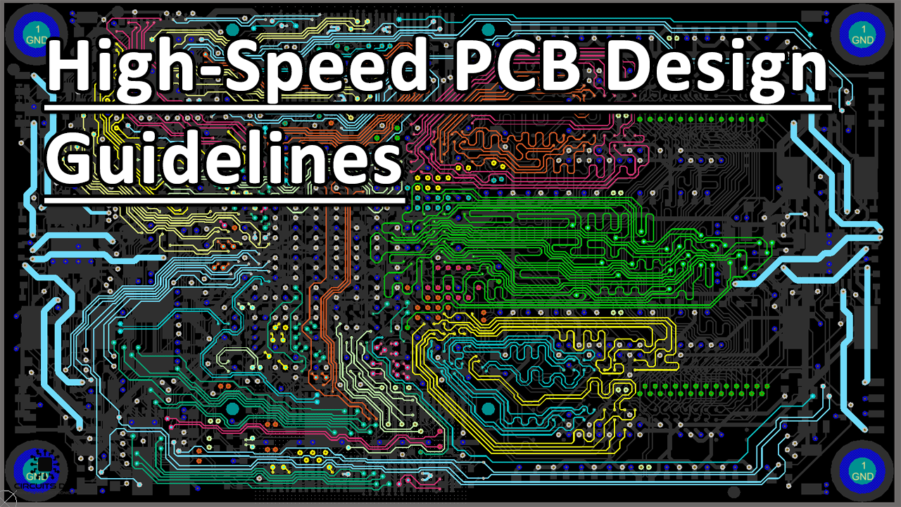
HighSpeed PCB Design Guidelines